We've updated publication list on our website, and reached a milestone! Feel curious to dive into more than 50 publications investigating Gallium Nitride power devices!

![]()
![]()
![]()
![]()
Our goal is the development of mature epitaxial GaN and AlN substrates. GaN-on-Si will obtain improved reliability by different epitaxial buffer structures. AlN will be re-grown on templates with high epitaxial quality. Finally, the correlations between material properties and device performance will be investigated.
From the lab:
News from 2020:
HEMT structures consisting of an Al 50 Ga 50 N channel layer and an AlN barrier layer have been regrown by MOCVD on top of the high crystal quality AlN/sapphire templates developed by the Japanese partners of the project (Mie and Kyushu universities). State-of-the-art performance was obtained for the transport properties of the HEMT, with a 2DEG electron density of 3.7e13/cm2 with associated mobility of 115 cm2/Vs resulting in a sheet resistance of about 1465 Ohm/sq. Devices made out of these epistructures exhibit current densities of 90mA/mm but with exceptional lateral breakdown voltages beyond 4000V.
News from 2019:
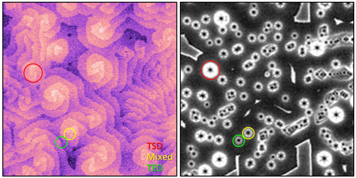 In the second year of the project, WP1 focussed mainly on the development and the understanding of the behaviour of GaN-on-Si buffer layer stacks designed for high voltage operation. On the one hand, carefully designed experiments allowed us to identify the contributions of the individual layers of a step-graded AlGaN-based buffer, especially highlighting the crucial role of the nucleation layer and its impact on the consecutively grown layers. By combining electrical characterisation and a variety of material characterisation techniques (e.g. defect selective etching in figure 1 as well as conductive atomic force microscopy, cathodoluminescence and X-ray reciprocal space mapping), we were able to find for the first time a direct evidence for the criticalness of extended defects within the buffer for high voltage operation of devices. On the other hand, we also developed a new buffer layer stack, based on strained superlattice layers, which show excellent leakage and trapping behaviour up to 1200V and at 150°C. In the second year of the project, WP1 focussed mainly on the development and the understanding of the behaviour of GaN-on-Si buffer layer stacks designed for high voltage operation. On the one hand, carefully designed experiments allowed us to identify the contributions of the individual layers of a step-graded AlGaN-based buffer, especially highlighting the crucial role of the nucleation layer and its impact on the consecutively grown layers. By combining electrical characterisation and a variety of material characterisation techniques (e.g. defect selective etching in figure 1 as well as conductive atomic force microscopy, cathodoluminescence and X-ray reciprocal space mapping), we were able to find for the first time a direct evidence for the criticalness of extended defects within the buffer for high voltage operation of devices. On the other hand, we also developed a new buffer layer stack, based on strained superlattice layers, which show excellent leakage and trapping behaviour up to 1200V and at 150°C. |
| WP1 also spent effort on the development of fully AlGaN- and AlN-based HEMT-structures, aiming to take advantage of the larger critical electric field compared to GaN-materials. We managed to grow HEMT-heterostructures with an AlGaN-channel layer and an AlN-barrier layer capped with in-situ SiN, with an electron carrier density as high as 2x 10¹³/cm2. In the next phase of the project, we will transfer the growth of these optimised heterostructures onto AlN-based substrate materials. |
News from 2018:
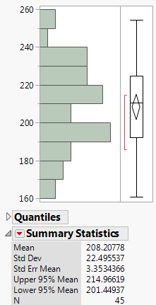 One of the aims of the project is to boost the performance of GaN on Si. Two strategies are employed: on the one hand by increasing the voltage handling capability, and on the other hand by reducing the on-state resistance. On a material level, the latter aspect is achieved by reducing the sheet resistance of the 2DEG by re-engineering the classical heterostructure that uses AlGaN barrier layers grown on a GaN channel layer. Two different approaches were investigated: ultrathin AlN barriers and lattice-matched InAlN barriers. The wafers with an InAlN barrier showed an exceptionally low sheet resistance with a median value of 208 Ohm/sq (distribution displayed on left figure). This value is roughly half the value of what is typically achieved with the standard AlGaN barriers. One of the aims of the project is to boost the performance of GaN on Si. Two strategies are employed: on the one hand by increasing the voltage handling capability, and on the other hand by reducing the on-state resistance. On a material level, the latter aspect is achieved by reducing the sheet resistance of the 2DEG by re-engineering the classical heterostructure that uses AlGaN barrier layers grown on a GaN channel layer. Two different approaches were investigated: ultrathin AlN barriers and lattice-matched InAlN barriers. The wafers with an InAlN barrier showed an exceptionally low sheet resistance with a median value of 208 Ohm/sq (distribution displayed on left figure). This value is roughly half the value of what is typically achieved with the standard AlGaN barriers. |
|
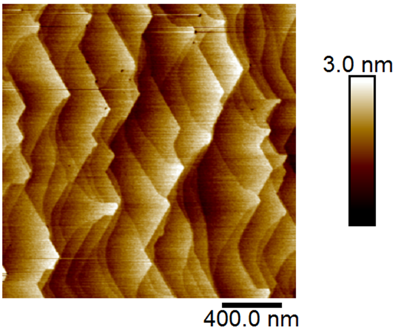
In order to explore the next generation of ultra-wide bandgap materials, the InRel-NPower project is exploring the AlN material system. A first step is to obtain very high quality AlN starting material onto which modified HEMT structures will be grown using MOCVD. Several types of AlN on sapphire templates have been provided by our Japanese partners in the project, Prof. Miyake and Prof. Kangawa from Mie University and Kyushu University respectively. These wafers were investigated in depth by project partners at Fraunhofer IISB in Erlangen and the University of Gent which indicated very high crystal quality (FWHM values below 60 arsecs for the 0002 reflection) and a very homogenously smooth surface with an RMS roughness value of only 0.35nm. Tapping-mode AFM measurements on AlN template substrate is displayed on the topography image on the left. The highly ordered morphology exhibits step edges in characteristic directions. |
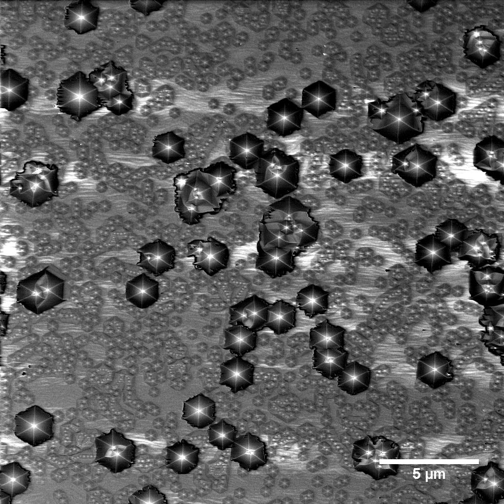 Fraunhofer IISB furthermore investigated the dislocation density of AlN templates by etching the surface with KOH/NaOH. The used etching parameters are optimized in a way that dislocation density can be determined in a reliable way, as illustrated in the picture on the right. Fraunhofer IISB furthermore investigated the dislocation density of AlN templates by etching the surface with KOH/NaOH. The used etching parameters are optimized in a way that dislocation density can be determined in a reliable way, as illustrated in the picture on the right. |
This project has received funding from the European Union’s Horizon 2020 research and innovation programme under grant agreement No 720527.