We've updated publication list on our website, and reached a milestone! Feel curious to dive into more than 50 publications investigating Gallium Nitride power devices!

![]()
![]()
![]()
![]()
Our goal of this last technical work package will be the development of two innovative packaging systems and two demonstrators in order to fully exploit the potential of the GaN devices.
From the lab:
News from 2020:


News from 2019:
|
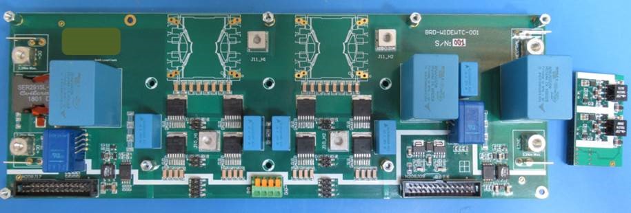
For realization of the DC2AC demonstrators first PCB’s are assembled and tested at hardware level with impedance check. Based on simulations implemented by OnSemi & CE+T of such triple half-bridge GaN based topology, the AC/AC efficiency shall go over 97% and 96% for DC//AC conversion. The IGBT has a switching frequency about 20kHz but GaN switches will be used advantageously at higher frequency, as far as it is advantageous to increase frequency. |
|
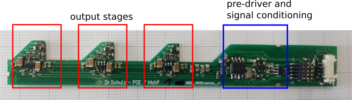
The first concept of the output stages for the motor drive inverter was realized with discrete MOSFETs (no integrated gate driver circuit), see figure above. The prototype was designed for three chips in parallel were each chip is driven by its own output stage. The pre-driver on the prototype ensures that no short currents occur in the output stages during the switching process. Furthermore, measurements for the output voltages on a passive (capacitive) load were executed and evaluated. |
News from 2018:
For packaging of the power modules two low inductive packaging concepts are developed: a pure ceramic material stack (BOSCH) and a planar ceramic-polymer concept (Siemens). In the double-sided ceramic module approach the GaN-power semiconductor will be surrounded only by typical ceramic circuit carriers. One basic advantage is here the inherent temperature robustness above 200°C for ceramic circuit carriers.
The surrounding of the chip from back and top side using ceramic LTCC-substrates (Low-Temperature Co-fired Ceramics) provides a special track design flexibility for a commutation cell and design flexibility of realizing or integrating the capacitor. By positioning a lower capacitor value quite close in a near-chip stepped DC-link design offers preferable low inductive effects while switching.
Towards the hybrid ceramic-polymer concept a compact interconnection technology replacing conventional wire bonding is being developed. For this purpose flexible planar metal interconnects on insulating layers are employed, providing the required low inductance. The concept of the technologies has been presented at a poster session (PCIM fair May, 2017, Berlin).
In comparison to state of the art vertical wide-band-gap SiC power devices even smaller pad geometries have to be handled by applying lateral wide band gap GaN power devices. Especially the application of the Ag-sinter process on all three-chip top-side pads is crucial.
In this context appropriate sinter paste material and sinter processes/ deposition have been developed. The comparative shear-test analysis on Ag-sinter pastes (Bosch-research-own/ commercial pastes) was successfully performed on LTCC dummy substrates. The results on SiC and Si-Chips suggest no obvious barriers for the planned Ag-sinter process of GaN-Chips on LTCC (see Figure 1).
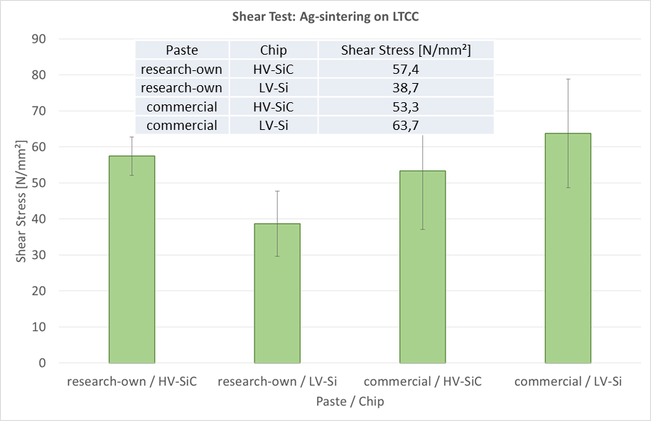
Figure 1: shear values of Ag-sintered dummy chips on LTCC substrate
For the both involved packaging technologies the pad configuration of the GaN Chips, the required top metallization as well as layout adaption for the assembly process have been designed.
This project has received funding from the European Union’s Horizon 2020 research and innovation programme under grant agreement No 720527.