We've updated publication list on our website, and reached a milestone! Feel curious to dive into more than 50 publications investigating Gallium Nitride power devices!

![]()
![]()
![]()
![]()
Our goal is the optimization and qualification of GaN-on-Si power device processing on a 6-inch pilot line while targeting on-resistance < 20mΩ for 650V applications. Furthermore, we will develop devices for beyond 2000V applications by optimizing the substrate-removal technique for GaN-on-Si technology as well as achieving novel power devices based on bulk AlN.
From the lab:
News from 2020:
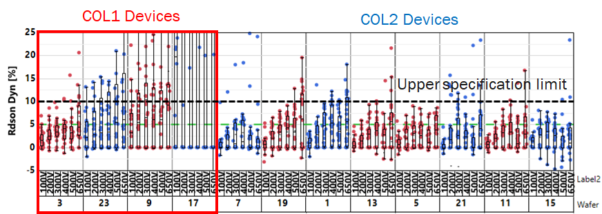
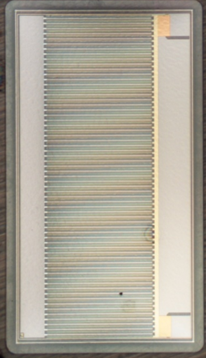
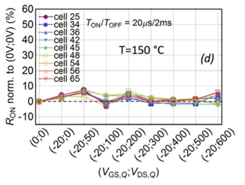
Dynamic On-resistance measurements comparing various normally-off device splits measured on a production tester (ON state: ~15 mSec; OFF state: ~100 msec) on 70 mm powerbars show the significant improvement throughout the project. The x-axis comprises of off-state quiescent voltage ranging from 100V to 650V with a step of 100V.
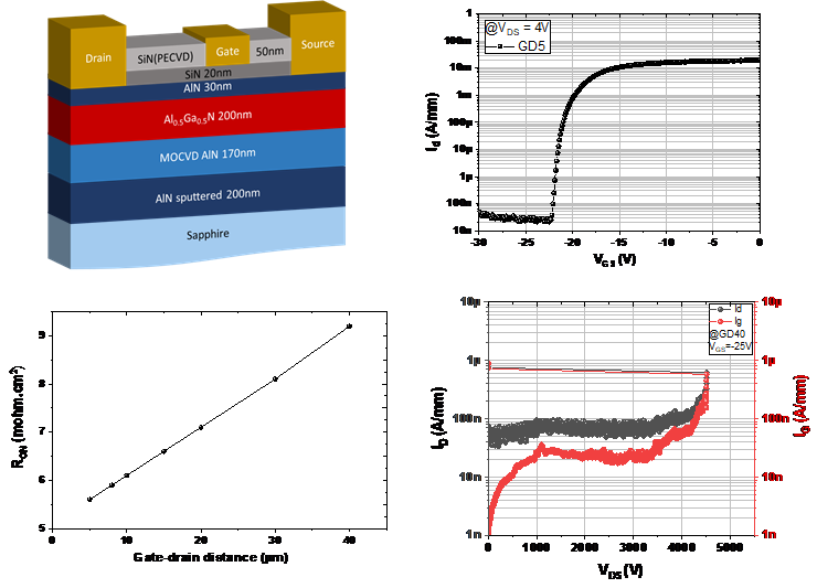
First AlN-based device demonstration with a successful fabrication of AlN/AlGaN/AlN double heterostructure delivering state-of-the-art 3-terminal breakdown voltage (BV) for AlGaN channel HEMTs with multiple kilovolts. These results show the potential of this material configuration for next generation high voltage power electronics.
News from 2019:
 The partner CNRS-IEMN successfully applied the local substrate removal approach on large devices representative of power applications fabricated by the company ONSemiconductor. Following the successful demonstration of the local substrate removal (LSR) technique on small proof-of-concept devices with a low leakage current and a three-terminal breakdown voltage of 3 kV, the objective is to apply this approach on large devices representative of power applications. A specific mask set has been developed in order to allow backside processing. This results in a direct comparison of devices with and without LSR on the same sample. Then, the samples have been thinned down to 170 µm and successful backside alignment and Si substrate full etching have been performed. Thick PVD AlN is being deposited on a first set of samples followed by a backside metallization, which will allow to evaluate the device performance in both cases. The partner CNRS-IEMN successfully applied the local substrate removal approach on large devices representative of power applications fabricated by the company ONSemiconductor. Following the successful demonstration of the local substrate removal (LSR) technique on small proof-of-concept devices with a low leakage current and a three-terminal breakdown voltage of 3 kV, the objective is to apply this approach on large devices representative of power applications. A specific mask set has been developed in order to allow backside processing. This results in a direct comparison of devices with and without LSR on the same sample. Then, the samples have been thinned down to 170 µm and successful backside alignment and Si substrate full etching have been performed. Thick PVD AlN is being deposited on a first set of samples followed by a backside metallization, which will allow to evaluate the device performance in both cases. |
News from 2018:
|
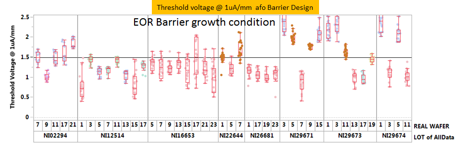
The partner ONSemiconductor significantly optimized normally-off GaN power devices in their pilot line with threshold voltages about +1.5V setting a new process of record. The threshold voltage variation is directly related to the variation of the barrier growth conditions. By tuning the growth condition of the AlGaN barrier and/or the related processing, the observed wafer to wafer variations can be attributed to the interaction between epitaxial growth conditions and processing. It must be pointed out that devices with high positive threshold voltages (> +2V) also suffer from turn-on issues (expected on-resistance not achieved for a specific gate drive). The various splits enabled both a positive threshold voltage (Vth > +1.5V) and also meets the RDS,on specification of 15 Ohm.mm (VG,on=+6V). |
|
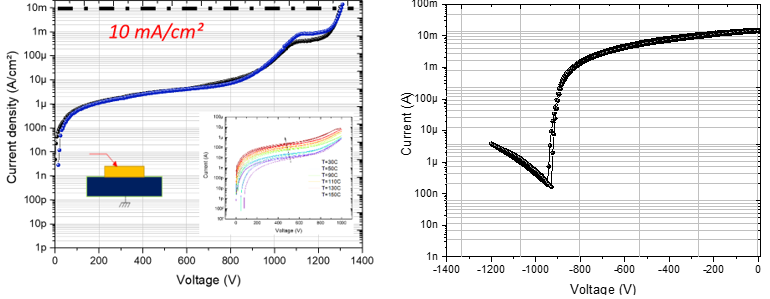
The partners EpiGaN and CNRS-IEMN have shown that the insertion of superlattices (SL) into the buffer layers allows pushing the vertical breakdown voltage above 1200V without generating trapping effects. Two buffer layers have been compared: one reference buffer without SL with a total thickness of 5.5µm and one SL-based buffer with a total thickness of 5µm. Vertical and lateral breakdown voltages have been measured at various temperatures. A vertical breakdown of 1300 V at 0.01 A/cm² is reached for the structure with SL compared to 1000 V for the more standard structure, even though the latter is slightly thicker. Furthermore, it can be noticed that a low vertical leakage current is observed up to a temperature of 150°C for the SL heterostructure. The effects of buffer traps have been studied through substrate bias ramp measurements using various sweep rates. The reference heterostructure without SL shows low trapping effect up to 800V with a strong trapping activation starting from 900 V. However, the optimized SL buffer uniformly delivers state-of-the-art low trapping effects all the way to 1200 V. |
Normally-on GaN-on-silicon power devices produced by the partner OnSemi with negligible dynamic-Ron both at room temperature and high temperature up to 600V have been demonstrated by Uni-Padova. This has been possible by the optimization of the influence of carbon doping on 2DEG concentration that needs to be minimized through proper optimization of the C-doping level. Furthermore, the thickness of the unintentionally-doped GaN channel needs to be properly tuned. Also, leakage through the unintentionally-doped GaN layer must be optimized in order to favor charge-redistribution through the structure (which leads to a complete suppression of dynamic Ron) without reaching an excessive vertical leakage current. |
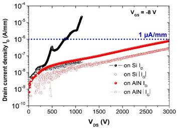 Best in class GaN-on-silicon power devices are currently limited by the buffer thickness in terms of breakdown voltage that cannot typically be grown above 6 to 7 µm, otherwise creating material defects or cracks due to the strain. This results in maximum lateral breakdown voltage below 2 kV. The partner CNRS has successfully developed a local silicon substrate removal technique to achieve state-of-the-art GaN-on-Si HEMTs with three-terminal lateral breakdown voltage of 3 kV. This achievement has been also obtained owing to the implementation of a thick high breakdown field AlN layer within the backside trenches followed by metal deposition to support the heat dissipation. Best in class GaN-on-silicon power devices are currently limited by the buffer thickness in terms of breakdown voltage that cannot typically be grown above 6 to 7 µm, otherwise creating material defects or cracks due to the strain. This results in maximum lateral breakdown voltage below 2 kV. The partner CNRS has successfully developed a local silicon substrate removal technique to achieve state-of-the-art GaN-on-Si HEMTs with three-terminal lateral breakdown voltage of 3 kV. This achievement has been also obtained owing to the implementation of a thick high breakdown field AlN layer within the backside trenches followed by metal deposition to support the heat dissipation. |
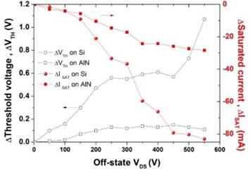 Finally, the partner CNRS also showed that current collapse characteristics of the substrate removed GaN-based MISHEMTs followed by thick PVD AlN and metal deposition were much lower as compared to reference devices (with silicon substrate).The double-pulsed ID-VG characteristics up to 550 V revealed significantly lower VTH shift and open channel current drop subsequent to high bias switching operation in the case of local silicon removal. These results indicate that in addition to the drastic blocking voltage enhancement, another key benefit provided by the local silicon removal approach is a lower current collapse owing to the removed interface between the AlN nucleation layer and the silicon substrate. Finally, the partner CNRS also showed that current collapse characteristics of the substrate removed GaN-based MISHEMTs followed by thick PVD AlN and metal deposition were much lower as compared to reference devices (with silicon substrate).The double-pulsed ID-VG characteristics up to 550 V revealed significantly lower VTH shift and open channel current drop subsequent to high bias switching operation in the case of local silicon removal. These results indicate that in addition to the drastic blocking voltage enhancement, another key benefit provided by the local silicon removal approach is a lower current collapse owing to the removed interface between the AlN nucleation layer and the silicon substrate. |
This project has received funding from the European Union’s Horizon 2020 research and innovation programme under grant agreement No 720527.